Printing With Light
How a 1957 lab experiment built the foundation for modern transistors

In the mid-1950s, the U.S. Army was working on ways to miniaturize “proximity fuzes,” the brains inside small munitions that signal to them when to explode. These fuzes were made operational by transistors, electronic switches that controlled the flow of current and which were new in modern electronics — having recently replaced bulky vacuum tubes. At the time, transistors were large and difficult to make — each one had to be made by hand, and humans were not precise enough to deliver a consistent product of the size required.
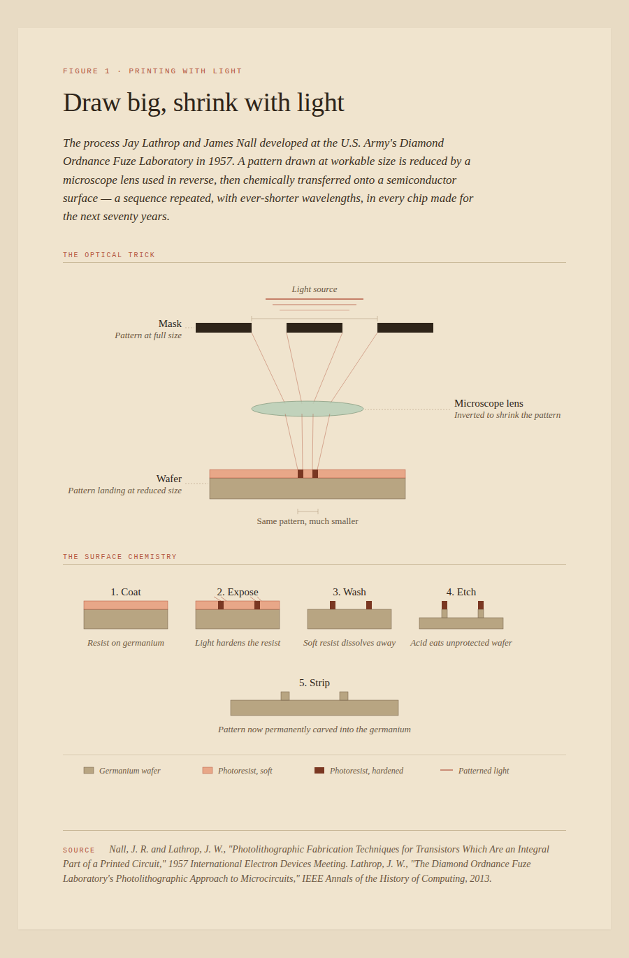
Jay Lathrop and James Nall, two scientists working at the Army’s Diamond Ordnance Fuze Lab, spent a couple of years exploring different ways to address this challenge. In 1957, they came up with an unusual insight, which was that the lenses on a microscope which normally made tiny objects appear large, could work in reverse — a larger object could be made tiny if viewed in the other direction.1 In other words, a transistor design of a workable size — the size of, say, a postage stamp — could be miniaturized using the flipped optics of a microscope. Earlier in the decade, Kodak had developed a liquid photoresist technology that if applied to a material, would harden when exposed to light. Lathrop and Nall tested their concept by coating a small wafer of germanium (the substrate of choice for early transistors — to be replaced by silicon years later) with Kodak’s photoresist, and exposing their transistor design pattern through the microscope eyepiece onto its surface. After a series of washes and chemical treatments, they had produced a patterned germanium surface — far smaller than any human could have produced — that could be further processed into a tiny transistor.2 They named their invention “photolithography.” The next step was to move their technique out of the lab and into the hands of those who could operationalize the process.
Because the entire semiconductor industry was searching for new ways to miniaturize transistors, the US Government — technically the owner of the technology — decided to allow Lathrop and Nall to share the details of the process with the major manufacturers, including Texas Instruments, RCA, Fairchild, and others. Shortly thereafter, Lathrop joined Texas Instruments, and Nall joined Fairchild — so the two inventors of the technology became part of the commercial push to build the next generation of electronics. By 1961, every major semiconductor company was using some form of photolithography in their manufacturing process, and each of them was searching for ways to make ever-smaller transistors. And the limit to this turned out to be the wavelength of the light itself.
During their experiments, Lathrop and Nall used the light that was available to them, which measured about 436 nanometers. A human hair is about 80,000 nanometers — so the light they used was about one two-hundredth of the width of a hair. Because the light is the actor on the photoresist surface, the wavelength of light determines how small the features of a transistor can be — which determines how small the transistor itself can be. Meaning, all else being equal, smaller wavelengths of light allow for smaller transistors. So the race was on to minimize the wavelength of the light used to make transistors.
By the early 2000s, wavelengths as low as 193 nanometers had been reached, and moving beyond this appeared to be physically impossible, for three reasons. At wavelengths below this level, the light was being absorbed by the surrounding air, and was thus not available to expose the photoresist. Second, the existing optics being used were not transparent for wavelengths this small, and thus could not direct the light properly onto the surface of the transistor substrate. And third, the photoresist needed to be chemically reformulated to work at lower wavelengths. These were each very difficult challenges individually. Together, they seemed insurmountable to the point where Intel, the largest and most profitable chip producer in the world at the time, opted out of committing to the next conventional step in photolithography, concluding that a radical leap was needed.
What was required was a completely new kind of machine that could incorporate extreme ultra-violet (EUV) wavelength light, focus it with a mirror-based optical system and pair it with a newly formulated photoresist. A single manufacturer was able to pull this off — a small Dutch company named ASML. They were not the logical favorite — Japanese companies Nikon and Canon were the largest manufacturers at the time, and ASML was a distant third. However, by working with a number of their suppliers and customers, ASML spent the next two decades and tens of billions of dollars solving each of these challenges. They ultimately built the newest technology using light at a wavelength of 13.5 nanometers — one six-thousandth of the width of a human hair. And their singular focus on addressing these challenges has been richly rewarded. Their newest machines, each costing $380 million, contain over 100,000 parts and require 250 engineers six months to install. ASML controls some 90% of the photolithography market and is the only company that can make EUV machines, an exceptional accomplishment.

The shrinkage in wavelengths has been accompanied by an equally remarkable growth in the number of transistors that can be placed on a given area of a chip. Specifically, ASML machines operating at a 13.5 nanometer scale can place 130 million transistors in a square millimeter — an impossible concept to grasp. If you counted one transistor per second around the clock, it would take over four years to get to that figure. And that is in each square millimeter. Transistors are electrical switches — a single transistor is just a switch, and not by itself very interesting. But when millions or billions of them are organized as part of a synchronized network, their usefulness is magical. Every operation performed on, say, a smartphone — sending a text message, taking a photo, listening to a podcast — engages billions of tiny transistors, flipping on and off in coordinated patterns to accomplish the task.

This has been a 70-year endeavor, with each seemingly unbreachable bottleneck being overcome, leading to layers of breakthroughs that are largely invisible. A user of AI is unaware of the underlying GPU, whose designer is unaware of the photolithography process, and on and on, back to Lathrop and Nall, who had the initial insight into how to make this all work. A largely invisible cumulative structure that undergirds our entire digitized world.
References:
One of my favorite childhood memories is 8-year-old me tying an AM transistor radio-a then recent birthday present, to the handlebars of my bike. To me, they had always been a “thing”. Interesting how cutting edge they actually were at the time! Good post!!